PCB is a heart for any modern electronic device.
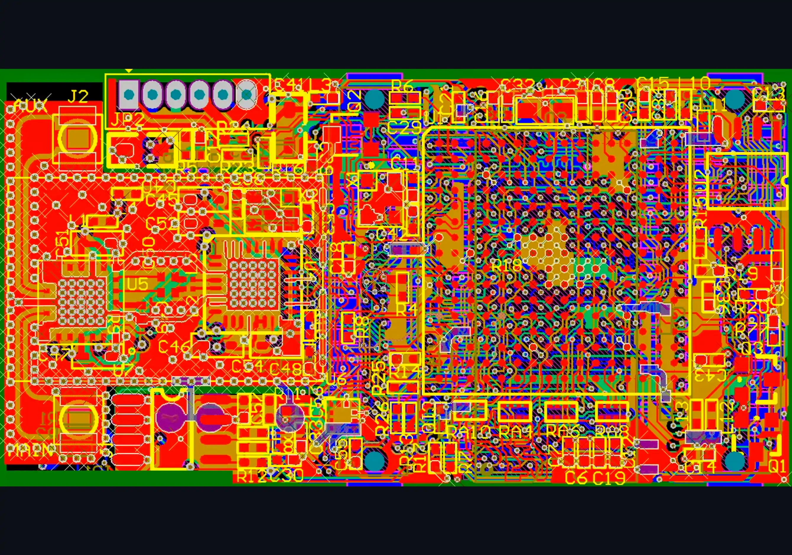
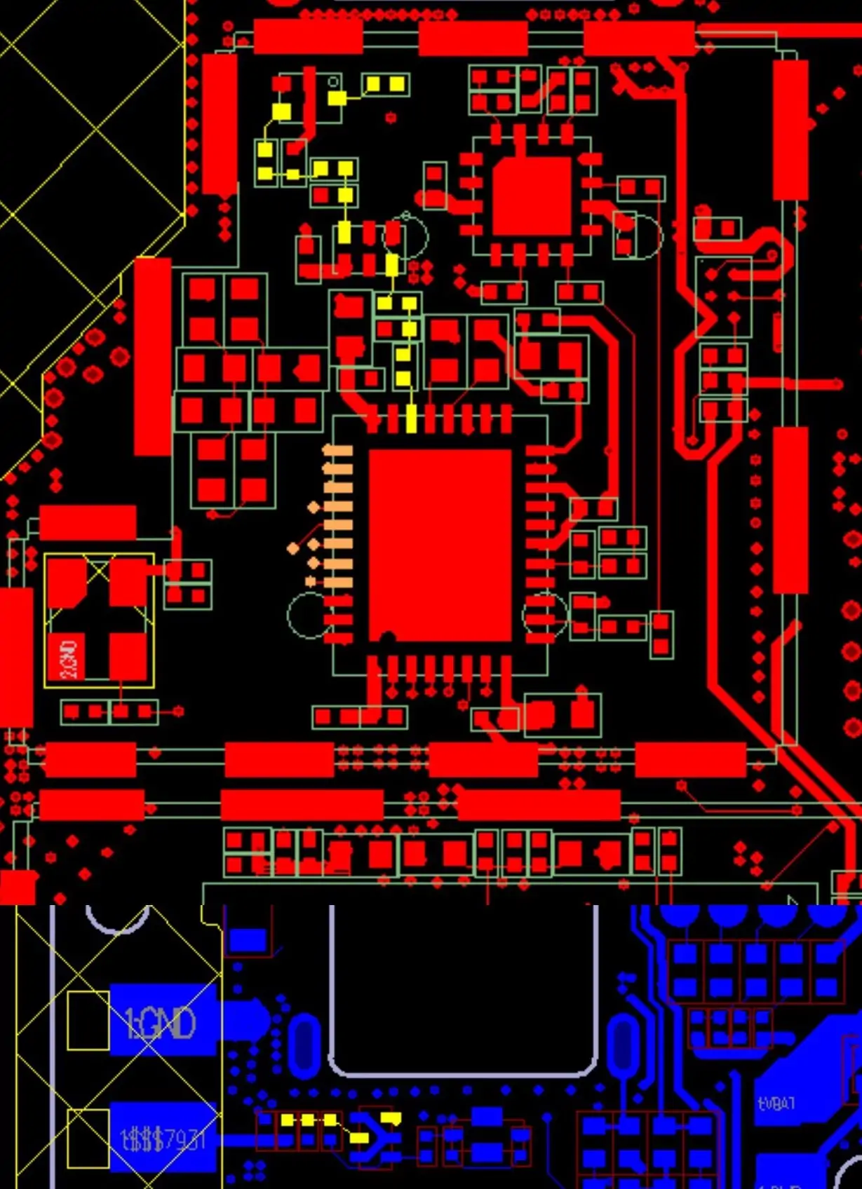
Almost any electronic device has at least one or sometimes several PCBs. PCB is a carrier for electronic components such as CPU/MCU or even SoC, memory, ADC/DAC, FPGA, LDO, DSP and many others depending on device type and application, PCB also normally carries memory and FW inside. PCBs carry many different components connecting them with copper rails, contact pads, connectors and other components located on them. Modern PCBs normally have several layers, and each layer includes thousands of rails connecting hundreds of components to each other. At the same time, it's important to reduce components, rails, and layers interference in order to keep information and signals pure. It also helps to increase reliability and operation stability.
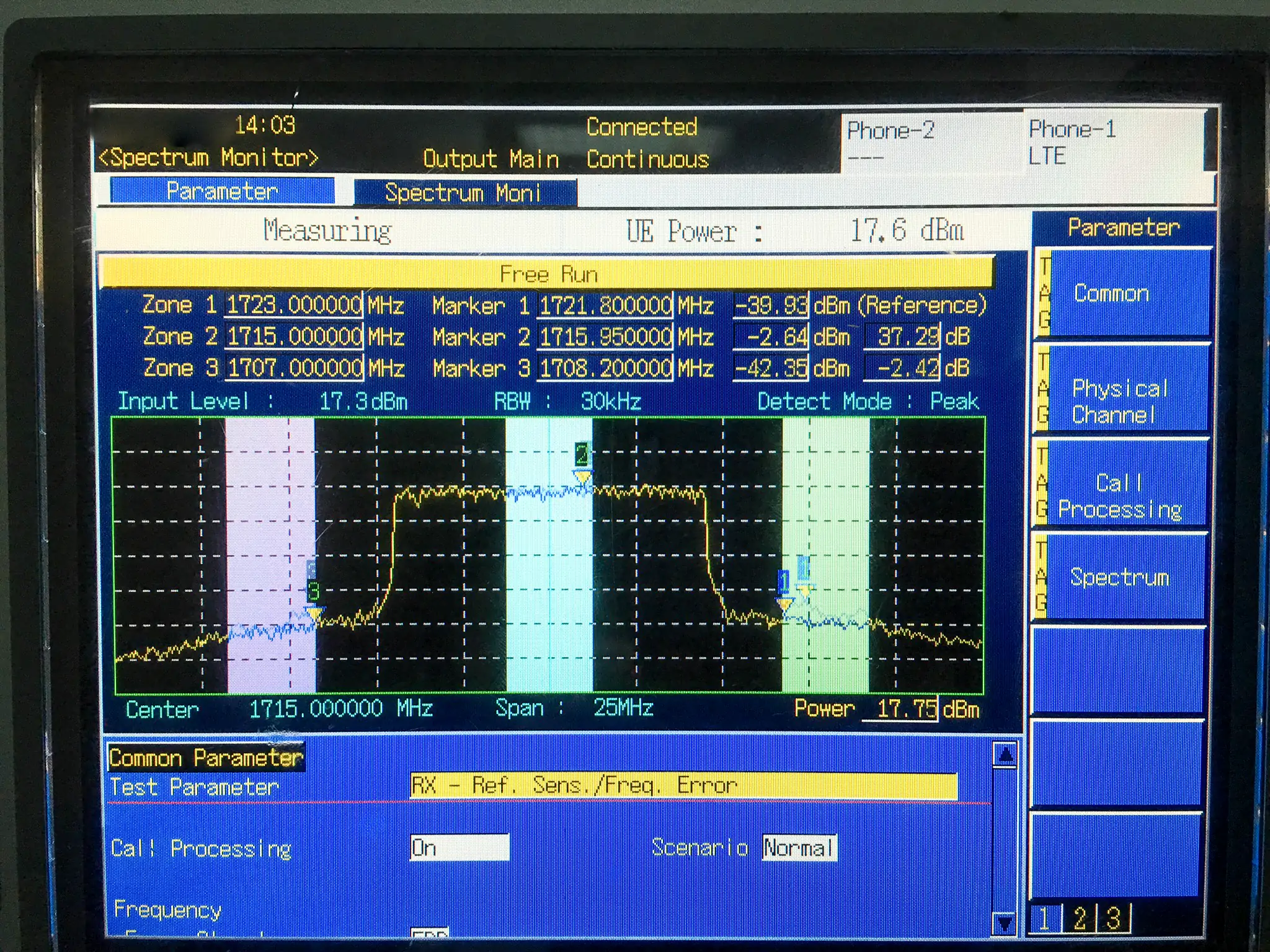
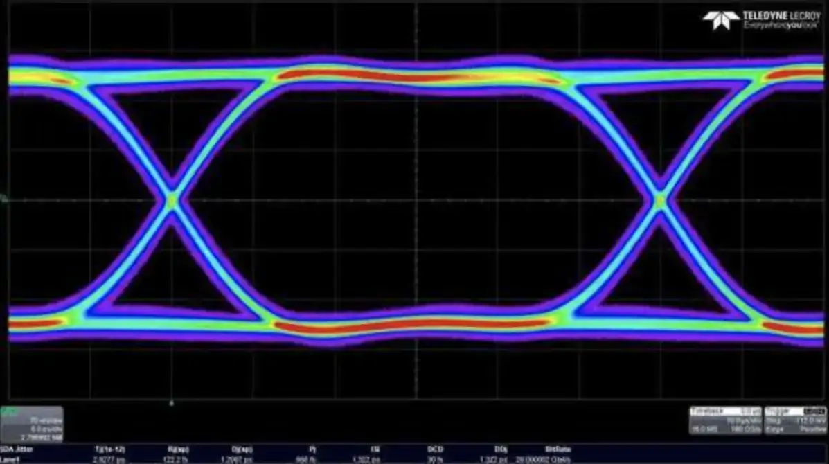
That's why PCB design is a complicated process and with increasing CPUs and memory speed, interfaces speed, and information volumes as well as 4G, 5G networks, DDR4/5, and nowadays even DDR6 memory it requires comprehensive and specific knowledge from engineers about signal integrity, interference, signals propagation and understanding which way to route signals, still no any automated routing SW can offer a robust solution for these challenging tasks better than a good engineer. Therefore, we are able to offer you the most experienced engineers who are able to handle these challenging tasks. From simple dual-layer PCBs to microwaves.
Hardware For Software is able to help you with the most complicated EE design for modern devices from microwave systems to servers. SoC/SiP/CPU selection, components End of Life analysis, BOM price optimization and components re-selection for your existing products, and many other factors allow us to create more competitive devices with lower BOM cost, reliability, and reduced Time to Market.
Almost any electronic device has at least one or sometimes several PCBs. PCB is a carrier for electronic components such as CPU/MCU or even SoC, memory, ADC/DAC, FPGA, LDO, DSP and many others depending on device type and application, PCB also normally carries memory and FW inside. PCBs carry many different components connecting them with copper rails, contact pads, connectors and other components located on them. Modern PCBs normally have several layers, and each layer includes thousands of rails connecting hundreds of components to each other. At the same time, it's important to reduce components, rails, and layers interference in order to keep information and signals pure. It also helps to increase reliability and operation stability.
That's why PCB design is a complicated process and with increasing CPUs and memory speed, interfaces speed, and information volumes as well as 4G, 5G networks, DDR4/5, and nowadays even DDR6 memory it requires comprehensive and specific knowledge from engineers about signal integrity, interference, signals propagation and understanding which way to route signals, still no any automated routing SW can offer a robust solution for these challenging tasks better than a good engineer. Therefore, we are able to offer you the most experienced engineers who are able to handle these challenging tasks. From simple dual-layer PCBs to microwaves.
Hardware For Software is able to help you with the most complicated EE design for modern devices from microwave systems to servers. SoC/SiP/CPU selection, components End of Life analysis, BOM price optimization and components re-selection for your existing products, and many other factors allow us to create more competitive devices with lower BOM cost, reliability, and reduced Time to Market.
- Our services:
- • architecture and schematic diagrams design
- • PCB routing
- • BOM optimization
- • PCB 3D-models design
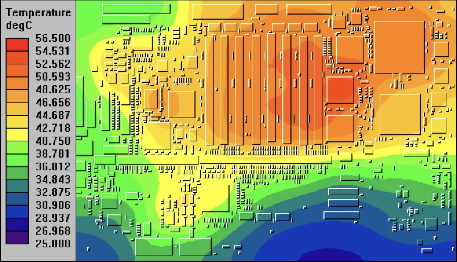
- • thermal modeling
- • signal integrity analysis(SI)
- • electromagnetic compatibility analysis (EMC)
- • power integrity (PI) and other related services on demand
Prototypes assembling in China and Georgia. Reliability, MTBF and other testing. Amendments upon testing results analysis.
Embedded FW development
- Supported architectures:
- • FPGA and SoC FW - VHDL and Verilog for Altera/Actel/Xilinx;
- • C/C++ FW for ARM, TI, TI DSP, ADI Blackfin, ADI DSP, NXP, Atmel, PIC, STM32, ATmega, MTK, Unisoc;
- • Bluetooth, Bluetooth Low Energy (BLE), WiFi, LoRaWAN, NB-IoT and other wireless front-end FW;
- • SW and FW development for Linux, Android other OS on demand.
Certification CE, FCC, EAC, RoHS, WEEE and others depends on your target sales area.
After project completion we providing all design documents for mass production according to industry common standards such as IPC, ISO and others upon your requirements. Average project lead time 3-4 month for middle embedded systems complexity for POC and EVT stages.We have reliable connections with MTK, Unisoc, FullHan, Lontium, TI and other semiconductor manufacturers, it allow us to have comprehensive support from them as well as information (include End of Life information) about latest SoC and other components.